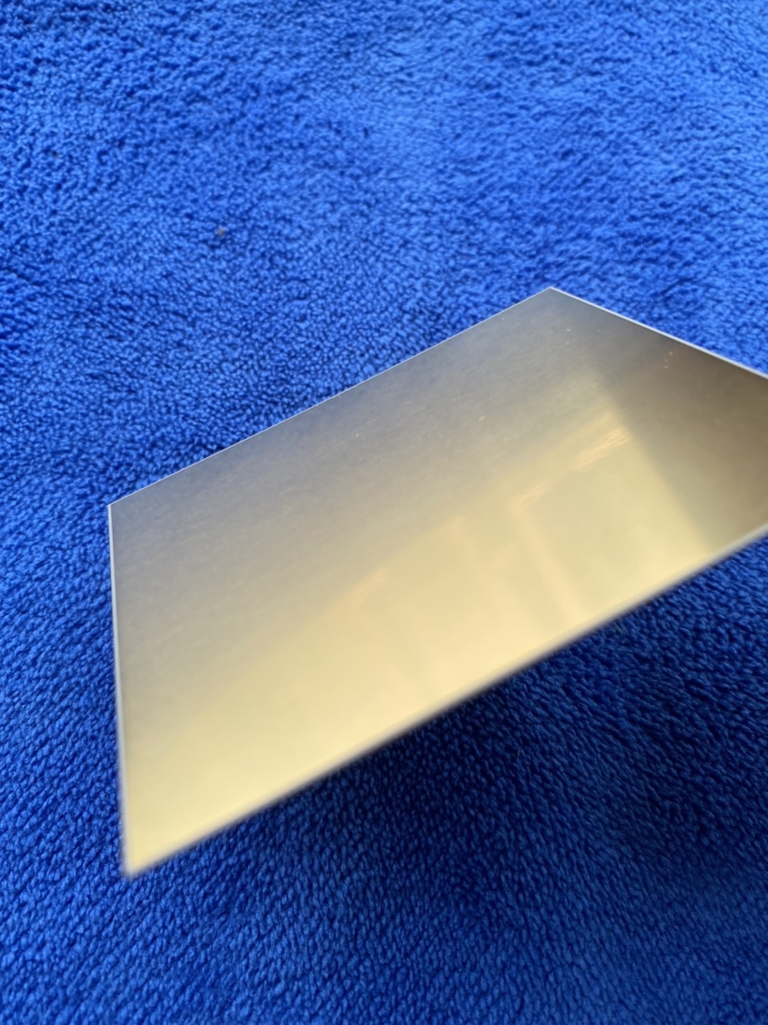
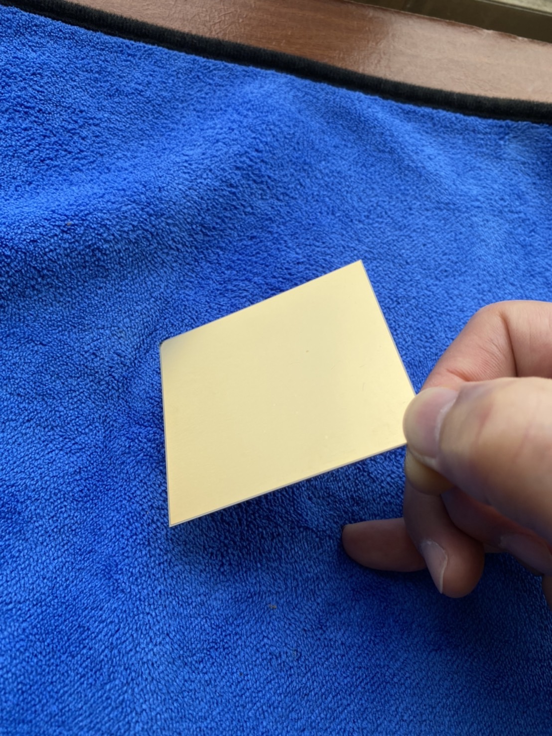
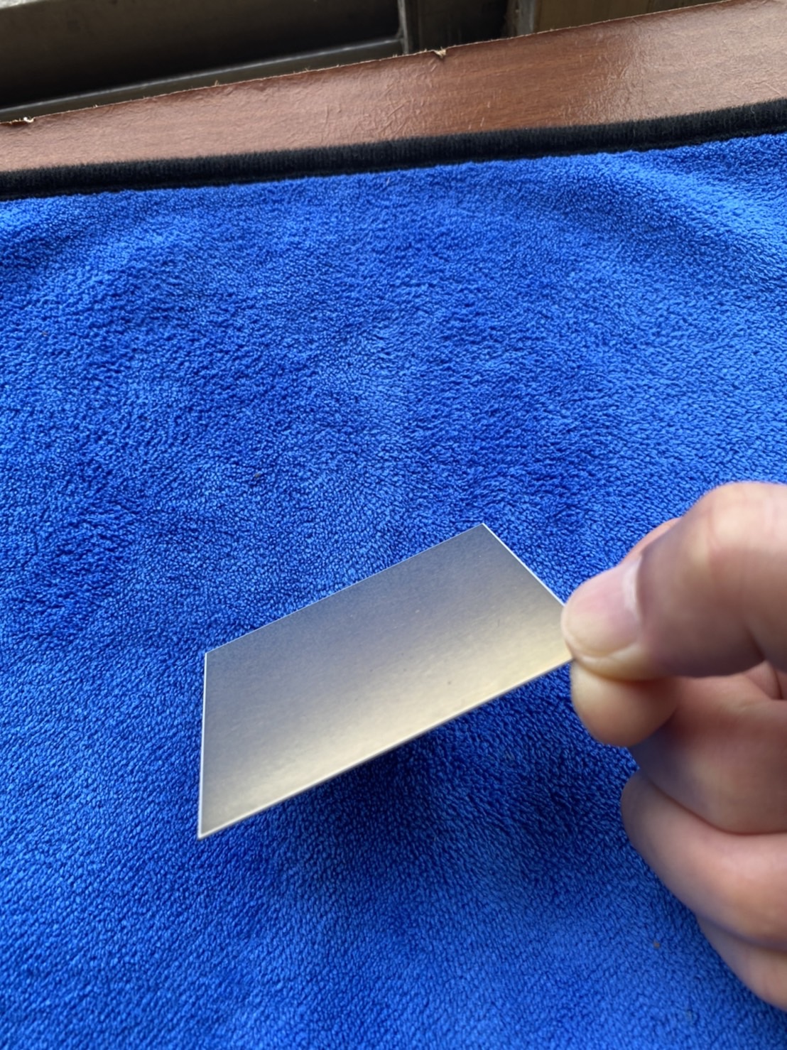
Silicon Nitride (Si3N4) printed circuit board (PCBs) coated with gold (full cover)
Peel Strength Test: 8.01 lbf/in
Solder Layer Thickness: 0.5 μm
- Fields:
- 1、Electric vehicles
- 2、Wind power generation
- 3、High voltage high power
- 4、Power electronics
- Applicable processing method:
- 1、Laser drilling
- 2、Laser cutting
- 3、A thinner solder layer can effectively enhance product quality and efficiency.
Silicon Nitride (Si3N4) printed circuit board (PCBs) coated with gold (full cover)
High-density silicon nitride gold-clad laminates are highly suitable for high-power and high-voltage circuit board requirements. The unique gold-clad process enables the perfect bonding of copper foil to silicon nitride substrate, effectively preventing delamination and significantly improving the yield rate of customer-side processes.
Nitride ceramic substrate has high hardness and strength, good thermal conductivity, low coefficient of thermal expansion, low high-temperature creep, resistance to oxidation and corrosion, low friction coefficient, and is a ceramic material with excellent comprehensive performance.
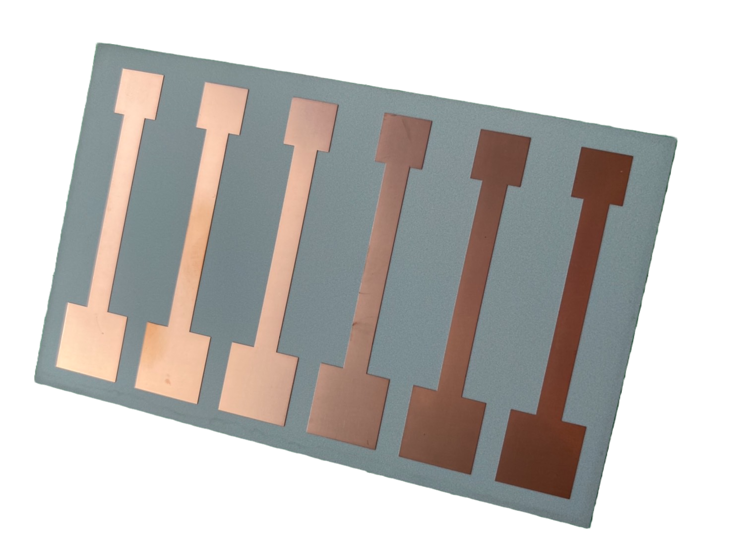
Test Result: Peel strength of the copper cladding reached up to 8.01 lbf/in
Silicon Nitride (Si₃N₄) Substrate with Copper Cladding – PCB Peel Strength Test
| Material | Copper Sample 1 | Copper Sample 2 | Copper Sample 3 | Copper Sample 4 | Copper Sample 5 | Copper Sample 6 |
|---|---|---|---|---|---|---|
| Si₃N₄ Substrate with Copper Cladding | 8.11 lbf/in | 7.74 lbf/in | 8.01 lbf/in | 8.19 lbf/in | 7.91 lbf/in | 8.07 lbf/in |
|
||||||
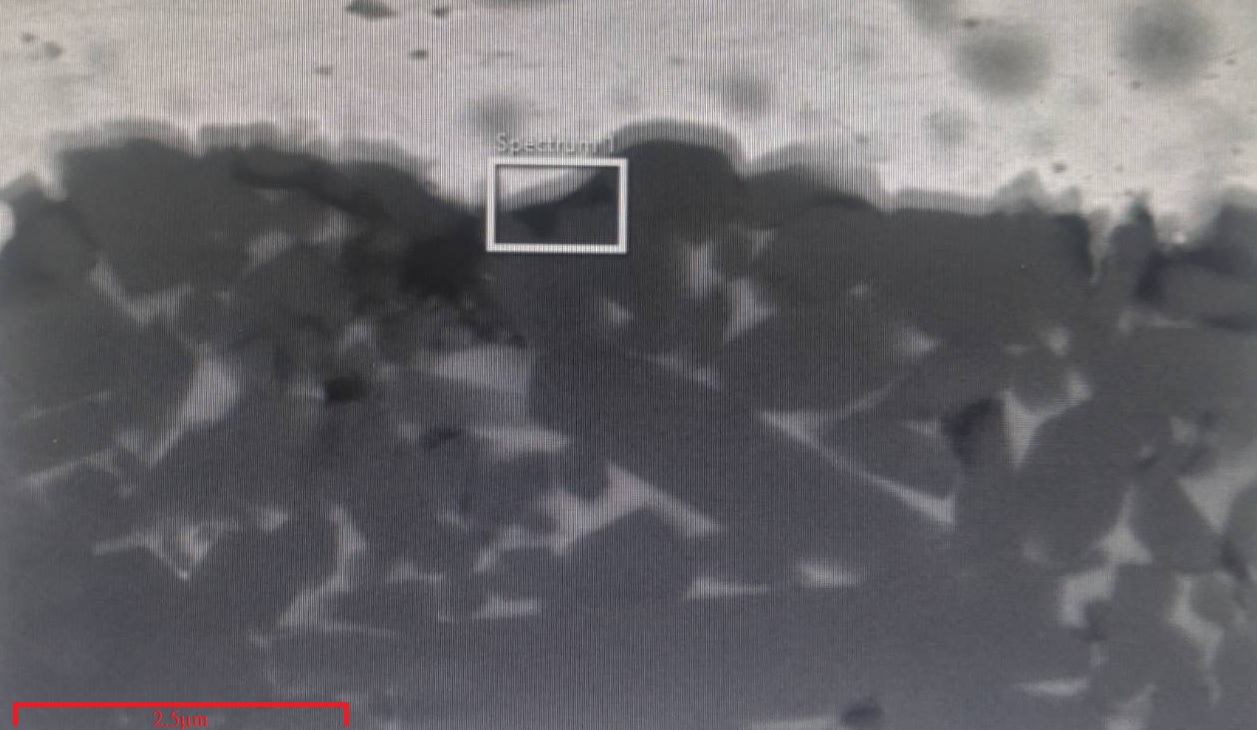
Advanced Copper-Cladding Process – Solder Layer Thickness: 0.5 μm
Cross-Sectional SEM Image of Solder on Si₃N₄ Substrate with Copper Cladding (Magnified 5000×)
|
High-Temperature and Thermal Cycling Test: Copper Cladding Remains Intact and Heat-Resistant
Si₃N₄ Substrate with Copper Cladding – 250°C High-Temperature Test
|
1. Place the board into an oven, heat to 150°C and hold for 30 minutes. 2. Continue heating to 250°C and hold for 90 minutes. 3. Without opening the oven, allow the temperature to drop to 80°C before removing the sample. 4. Check for warping of the substrate and delamination of the copper cladding.
Test Results:
|

|
Technical Specifications – Si₃N₄ Ceramic Substrate
| Item | Unit | Test Standard |
|---|---|---|
| Color | Off-white | |
| Density | g/cm3 | 3.2 |
| Flexural Strength | MPa | >800 |
| Camber | Length % | ≦3 |
| Thermal Conductivity | 25°C, W/(m·K) | >80 |
| Coefficient of Thermal Expansion |
10-6/K (40–400°C) 10-6/K (40–800°C) |
2.0–3.0 2.0–3.0 |
| Dielectric Strength | kV/mm | ≧17 |
| Volume Resistivity | ≧1014 Ω·cm |
AMB copper-clad silicon nitride Si3N4 circuit board
| Item | Unit | Test Standard |
|---|---|---|
| Plating Temperature Resistance | Custom copper thickness | 410±10°C, 5 minutes |
| Solder Mask Temperature Resistance | 320°C, 60 seconds | |
| Thermal Shock | (0.32 mm Si₃N₄ / 0.3 mm Cu), no via, -40°C to 150°C, transfer time <30 min; >3000 cycles |
|
| Surface Roughness | μm | Ra ≤ 1.5 μm |
| Peel Strength | N/mm | (50 mm/min) |
| Solder Wettability | % | ≥95 (Sn/0.7Cu) |
| Void Content (C-SAM) | ≤3% |
Product Specifications
| Item | Unit | Test Standard |
|---|---|---|
| Thickness |
0.254 mm 0.32 mm 0.635 mm 1.0 mm |
|
| Length × Width |
114.3 × 114.3 mm 138 × 190 mm |